Simba GaoMECHANICAL / MECHATRONICS
← All projects

CARNEGIE MELLON / MEMS DESIGN / 2025

Theoretical Design and Fabrication of a Cavity-Based MEMS Faraday Cup

I designed a two-wafer Faraday-cup concept with a 22 µm aperture, balancing charge retention, signal collection, and fabrication constraints.

My role Device geometry, fabrication-process design, and structural analysis · four-person team.
  • MEMS design
  • Microfabrication
  • Structural FEA
  • Analytical modeling
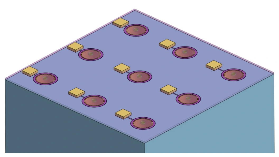
CAD concept of a nine-cup MEMS array with small apertures and contact pads.
Array concept · theoretical design and proposed fabrication
22 µmAperture diameter · final sizing study
350 µmCavity depth · final sizing study
2 wafersProposed bonded structure

01 / ENGINEERING PROBLEM

Balance charge collection and fabrication

The goal was a microscale Faraday cup for measuring ion-beam charge. A covered cavity limits secondary-particle escape, but a smaller opening also reduces incoming signal and complicates fabrication. I worked on the geometry, process sequence, and aperture-plate strength to make that tradeoff practical.

02 / METHODS & ANALYSIS

Geometry, process, and structure

Design schematics and simulation figures
Click images to enlarge

01

Size the aperture and cavity

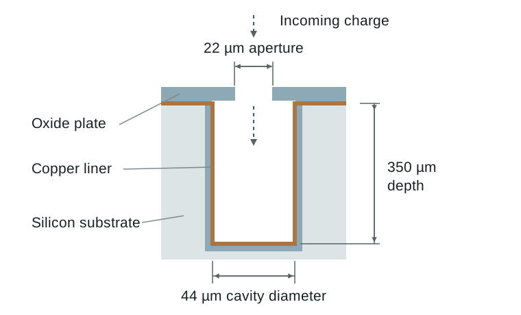
Final sizing schematic: 22 µm aperture, 44 µm cavity diameter, and 350 µm depth; not to scale.

Final report sizing · schematic, not to scale

Smaller apertures suppress escaped charge but also reduce incoming signal. I used the report’s beam assumptions and a 1 fA readout noise floor to size the aperture, then selected a cavity diameter that relaxed the internal coating aspect ratio to approximately 8:1.
02

Develop a two-wafer fabrication process
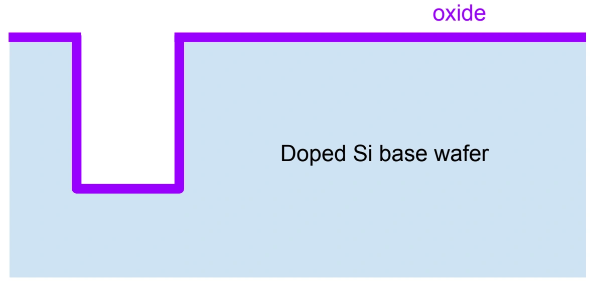
Proposed cavity wafer after deep reactive ion etching and growth of insulating oxide.
01 Etch the cavity and grow oxide
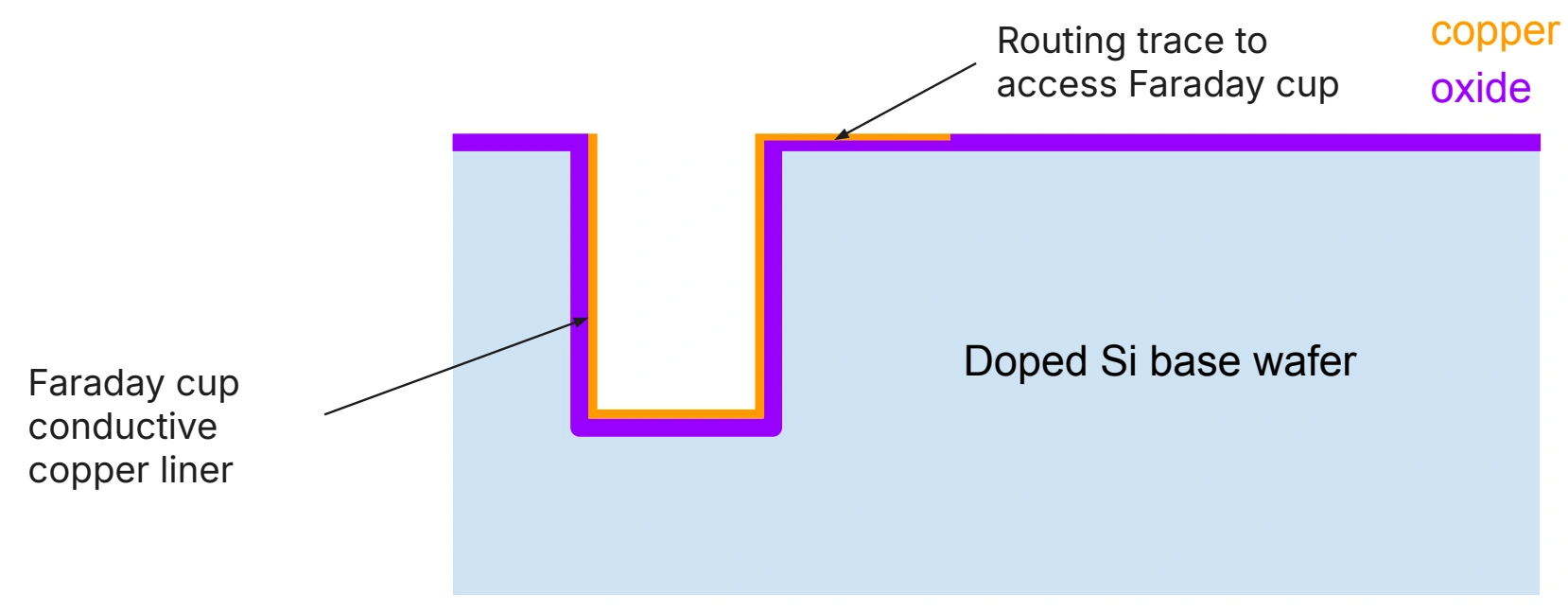
Copper liner and routing trace after conformal deposition and polishing.
02 Deposit copper and polish the surface
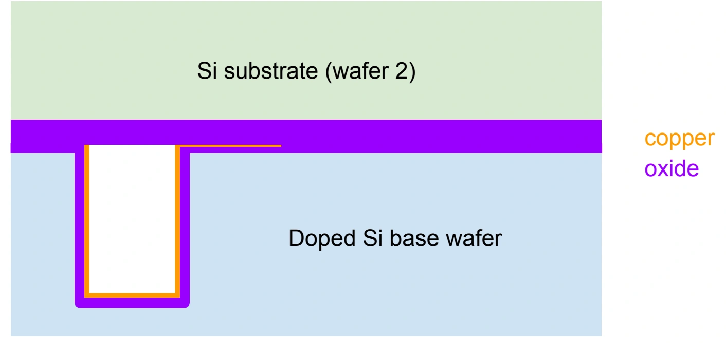
Aperture wafer bonded above the copper-lined cavity.
03 Bond the aperture wafer at 200–250 °C
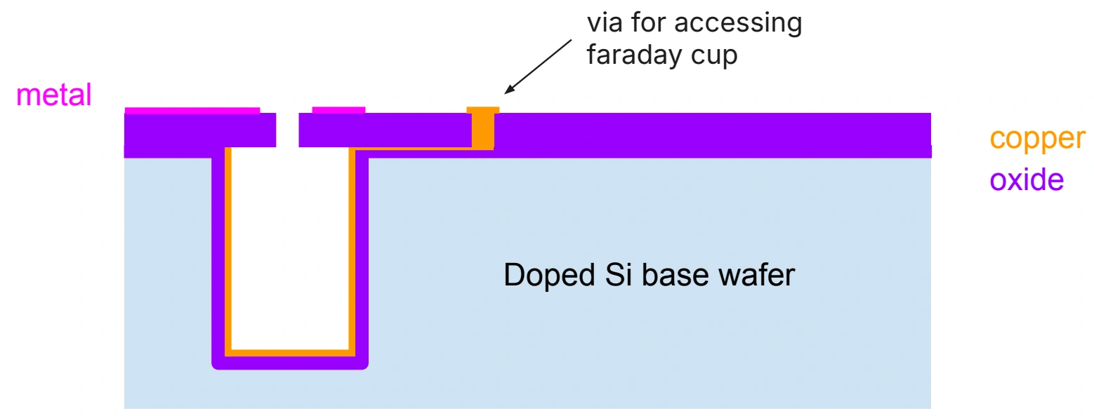
Finished process concept with an aperture, suppressor electrodes, and a top-side contact via.
04 Open the aperture and form contacts

I proposed separating the cavity and aperture wafers so the deep cavity could be etched and metallized before sealing its narrow opening. Low-temperature oxide bonding limits copper diffusion; subsequent patterning forms suppressor electrodes and accessible contacts.

03

Check the aperture plate under resist loading
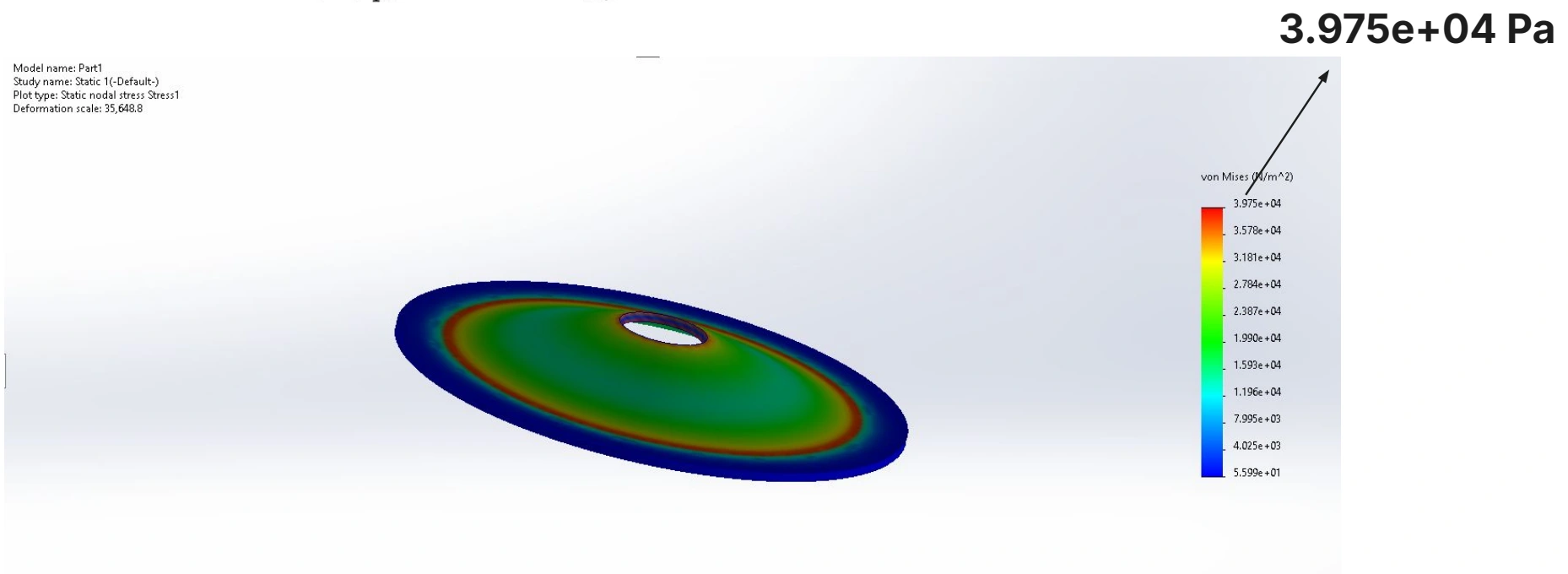
Preliminary aperture-plate FEA showing a peak von Mises stress of 3.975e4 Pa under the assumed photoresist loading.
EARLY PLATE MODEL
50 / 5 µmPlate / opening diameter
1–10 µmAssumed photoresist thickness range
39.8 kPaPeak von Mises stress · simulation
I compared plate-bending calculations with FEA to screen the aperture plate under assumed photoresist loading. This preliminary case used an earlier geometry; residual stress, bonding, and pressure loads still need evaluation for the final design.

03 / RESULTS & OUTCOME

A defined design and fabrication route

ANALYTICAL + SIMULATED · NOT FABRICATED
≈99.9%Idealized geometric collection estimate
22 µm aperture · 350 µm depth

The geometry study and two-wafer process define a candidate design, not measured collection performance. Next steps are bonding and stress checks on test structures, followed by leakage, capacitance, and charge-collection measurements on fabricated devices.
Team electrical-model cross-check
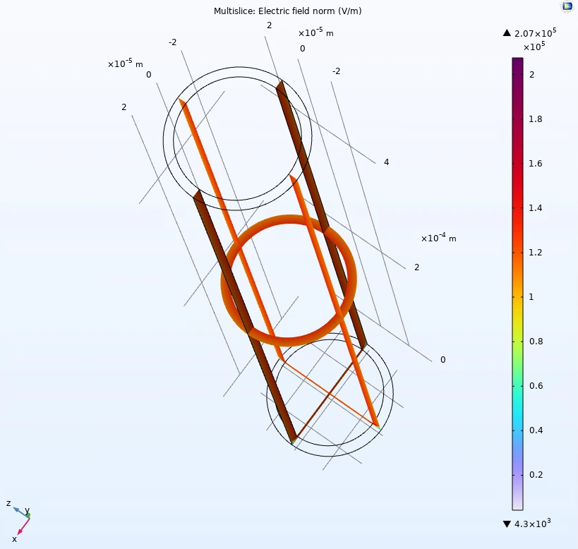
Team COMSOL electrostatic model used to calculate cup-to-ground capacitance.
Team COMSOL model · separate electrical-analysis geometry

Cup-to-ground capacitance

792 fFAnalytical model
816.4 fFCOMSOL

The team’s electrical model differed by approximately 3.1% from its analytical estimate. This cross-check used a separate 63.5 µm-diameter, 500 µm-deep cavity with 5 µm oxide.